Physics 429: Practical Exercise
This mandatory exercise will guide you some of the available technologies and refresh you on some skills that will play a key role completing the experiments in Phys 429. The premise of the exercise is as follows: you are measuring a very weak signal from a distant star which you expect to be a pulsar. Unfortunately, the signal is so weak that it must be greatly amplified leading to a very low signal to noise ratio (SNR ≪ 1). By looking in the frequency domain however, it is apparent that the signal of interest exists in a narrow region of frequencies, whereas the noise is spread across a very wide frequency band. Your task is to devise a filter which can isolate and amplify the signal, yeilding a much higher SNR.
Practically, your task involves three stages: first you will design a filter on paper and test it on a breadboard. After you are convinced that your design works the second stage will involve soldering up a permanent device which can be placed in an experiment. Finally, for the third component of the exercise, you will design and 3D print a protective enclosure for your device with input, output and power terminals.
Electronics Portion
You are to design a suitable filter capable of dramatically improving the signal to noise ratio (SNR) of the signal.
Input and Output Impedance: Buffering Your circuit
When measuring a signal in the lab we often work under the assumption that the measurement we are making does not affect the signal we're trying to measure. Unfortunately this is never the case, but with good practice, a measurement device can be made to have a negligable effect. The primary effect of a measurement on a signal is known as loading error which can be understood as follows: An ideal voltage source is a device that creates a fixed potential difference between its terminals no matter what. Even in the limit of zero Ω of resistance between the terminals and therefore infinite current, the voltage remains fixed. Obviously this can't work in practice (among other reasons, since power P = iv this would require infinite energy). In reality real voltage sources can only supply finite current, a fact that can be modelled as an ideal source in series with an internal resistance Rs.
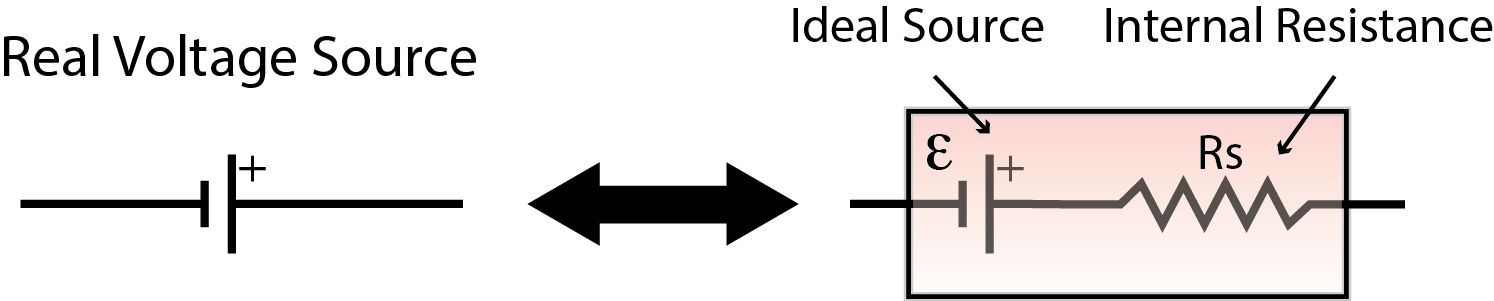
Then when the supply is short circuited there is a finite current that can flow: i = V/Rs.
This leads directly to the phenomenon of circuit loading, for suppose that we now hook something (typically called a "load", with some resistance RL to our real source):

This new circuit now forms a voltage divider with the internal resistance giving voltage:
$$ v_\text{real} = \frac{R_L}{R_{int}+R_L}v_\text{ideal} $$i.e. We will measure a different voltage than is actually provided (without measurement)!
We see that the optimal value for Rint is 0Ω and as long as Rint ≪ RL, there will be neglible loading error. In practice we can never make it zero but we can make it very small. RL is an example of "output impedance".
But what if are given an device with a poor, or unknown output impedance? Is there a way to "lower it". It turns out there is a way to do this by using active electronics (typically transistors or opamps) to form what is known as a buffer stage. There are several ways to achieve a buffer but the prefferable method in most cases is to use an (op-amp) operational amplifier.

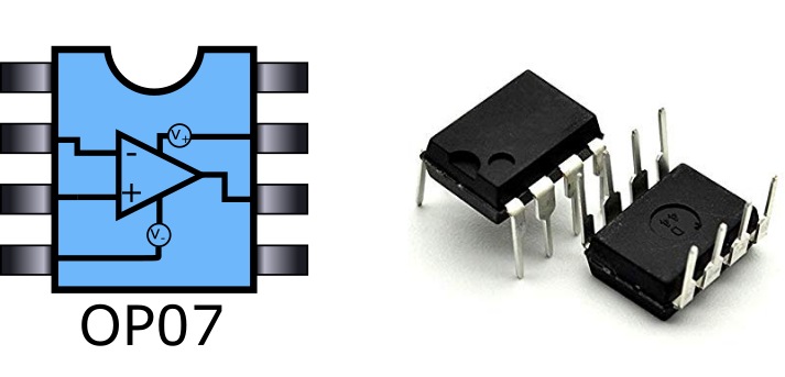
This is the symbolic representation of an opamp of course. The devices you will use are in a integrated circuit package:
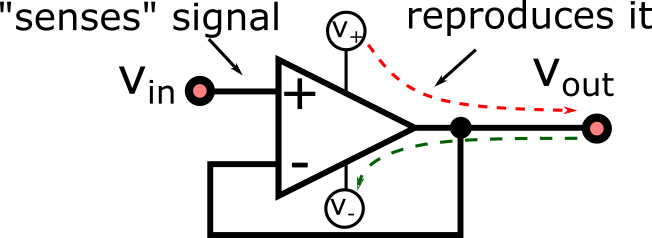
Recall that an opamp is really just a very high gain differential amplifier with favorable properties. First, they are constructed so that they have a very high "input impedance" typically tens of MΩ up to GΩ This effectively means that they draw very little current at their inputs. This leads to the so-called "First Golden rule of opamps":
The "second golden rule of opamps" stems from their very high differential gain. In fact the gain is so high as to make the opamp almost useless if used directly as a differential amplifier, but is extremely useful when used in negative feedback configuration. When used in negative feedback, the output has a stable value only when the input terminals are very nearly equal - any deviation from this leads the output to swing back towards the stable point. This is just a statement of negative feedback but is so important in understanding opamp design that it gets its own golden rule:
We can use these golden rules to understand the operation of a buffer op-amp:

From golden rule #1, the inout draw's no current. Thus RL → ∞ and the loading error is therefore negligable regardless of RL of the source. From golden rule 2, vout = v+ = vin. This circuit thus reporduces the input signal but without loading and the very low output impedance of the opamp. This buffer also serves as a circuit protector, for if we short circuit something after the buffer, all the current comes from the supply and whatever we've plugged into vin is unaffected.
Everything that we've discussed is for voltage sources but we're making filters and signal generators. Recall from your second year instrumentation class however that there is a principle known as Thevenin's theorem that says that in any linear circuit, according to any two nodes within that circuit the rest of the components, regarless of their complexity act identically to a real voltage source with some ideal voltage (the Thevenin voltage vth) and some internal resistance (the Thevenin resistance Rth). You can dust off your electronics book now if you want to see how to calculate those quantities. All this is to sat that the circuits we are analyzing will have some input impedance which we want to be large and some output impedance that we want to make small.
For this exercise you are required to make a buffer stage before your filter, for the reasons outlines above.
Filters and roll-off
An incredibly useful fact of electronics is that we can generalize Ohm's and Kirchhoff's laws and everything that comes from them to any linear element by incorporating its complex impedance at a given frequency ω. For a resistor the impedance is simply ZR = R. For a capicitor ZC = -j/ωC where we're using j instread of i for the square root of -1 (i is current so things get very confusing very quickly if we use i for imaginary numbers too!). Finally, an inductor has ZL = jωL. If we use these values, we still have v(ω) = i(ω)z(ω) and the voltage divider equation still works!
$$ \frac{v_{out}}{v_{in}} \equiv G(ω) = \frac{Z_2}{Z_1+Z_2} $$For example, consider the following "RC" circuit with Z1 a resistor and Z2 a capacitor. Plugging the equations into the generalized voltage divider equation yeilds:
$$ G(\omega) = \frac{1}{1+j\omega RC} $$The gain is thus different at different fequencies. At DC (ω → 0) G = 1 while at very high frequencies (ω → ∞), |G| → 0. The cross over bewteen low and high frequecies roughly occurs where the real and imaginary terms in the denominator are of equal magnitude, i.e. at the "cut-off frequency", where
$$ \omega = \omega_{co} = \frac{1}{RC} $$When we plot the magnitude of the gain, in decibels on a semilog plot vs frequency, we form what is known as a Bode plot for the filter. Recall that for voltages, the gain in decibels is:
$$ G_{dB} = 20\log_{10}\left[G(\omega)\right] $$Often the phase of the gain is also plotted:
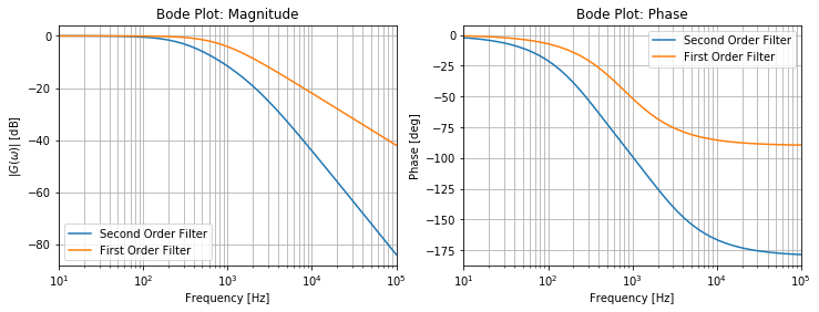
Note that when the term ωRC ≫ 1, the gain is purely imaginary (φ = -90o) and the magnitude obeys a linear relation on a semilog scale.
$$ G_{dB} = -20\log_{10}\left[\omega\right] + const $$This slope of -20 dB/decade (a decade is a power of 10) is called the roll-off of the filter. Note that this means that we don't have a "brick-wall filter" that completely rejects everything above the cut-off and transmits everything below it. Such a filter, although ideal, would in fact be impossible. By cascading several filters or combining them in more sophisticated topologies however, we can greatly improve on the steepness of the roll-off. Two filters, back to back, for example can create roll-off of -40 dB/decade and three can make -60 dB/decade.
Soldering
Having tested your circuit on a breadboard, you will now manufacture a more permanent version of your device using a prototyping board and soldered-in components. The protoboard includes wire terminals placed on an insulasting surface:

In this type of construction, the electronic components are permanently fixed into position, resulting in a much more reliable assembly. There are many tricks of the trade employed by skilled technicians, but with a bit of practice and a few principles, you can learn to do enough basic soldering to rapidly prototype your own designs.
It is best to layout your design physically by placing the components on the board and copy this layout on to paper before starting. To solder a component, it is best to hold the soldering iron like a pen, taking care not to touch the tip or any of the metal areas near it. Gently place the tip of the iron onto the joint to be soldered. The tip should contact both the component wire as well as the circuit board pad.
After waiting a few seconds for the metal to heat up, feed some solder in to the joint.

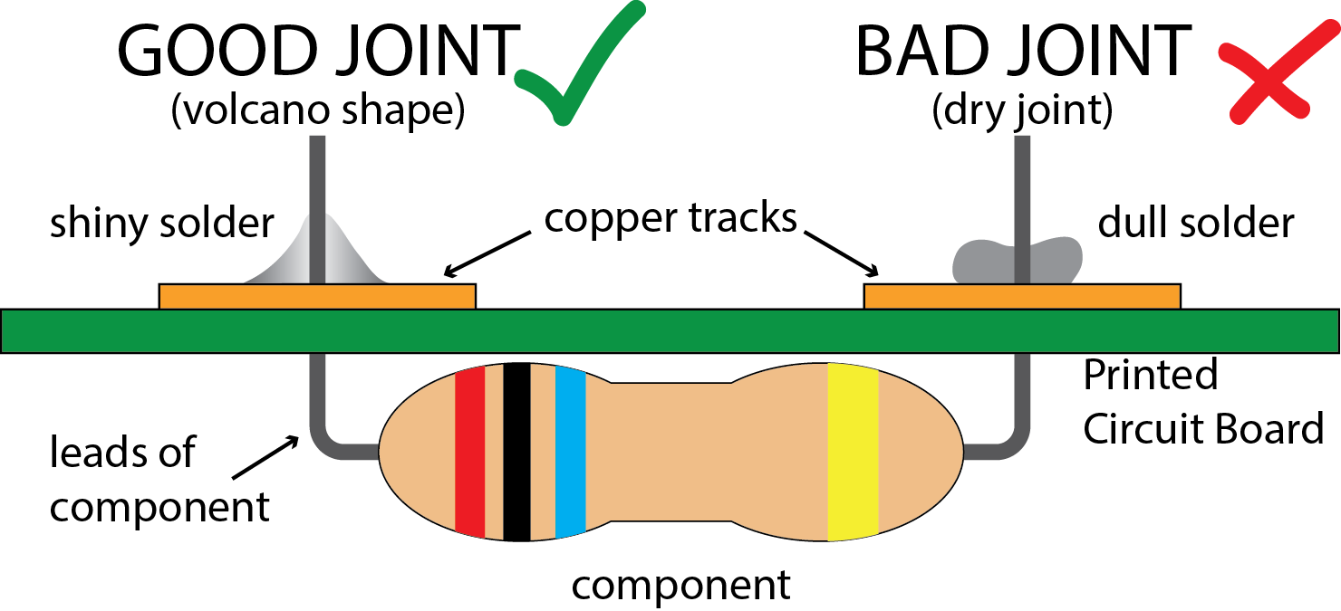
It should melt and immediately flow onto the trace and around the lead forming a “volcano” shape. If this is not happening, it usually means the joint is not hot enough. Let the joint cool off for a few minutes before trying again.
After you have soldered up your component, it is time to test it out. Before doing this, carefully trace the circuit and verify all the connectionsare where you intended, it's easy to overlook a ground connection, or have a glob of solder unintentionally connecting two wires. If everything looks good, you can power it up and verify that it works as intended. If it does, great. Time to move on.
BUT WHAT IF IT DOESN'T?! This is not a huge problem. The first step is to walk though circuit, from the input to the output. At some point, things will have gone south. Concentrating on this region you can likely spot the problem. You can then remove any errant connections using solder wick provided and resolder the component, starting the debugging section again. If a component became damaged in the process, don't worry - we have plenty of replacements! Just ask your instructor.
Mechanical Portion
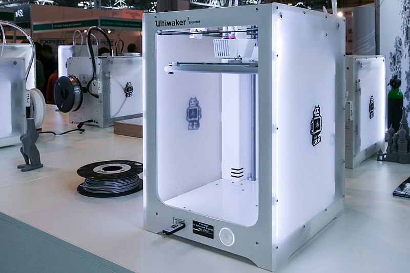
Having designed, breadboarded and soldered (and tested!) your circuit, it needs to be placed in an enclosure, i.e. a box containing your circuit with input, output, an power cables. Our approach will be to 3D print an eclosure, leaving panel cutouts for signal (BNC cables), and power (banana jacks). As a Phys 429 student, you have access to our Machine Shop's Ultimaker 3, 3D printer:
Of course before you print it, you must design it. To do so, we recommend that you use Fusion 360, a professional, high-end CAD (computer aided design) software package which is freely available to students. To get started, install F360 on your own system (if this is not possible, see me!).